


Video
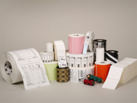
Wave Soldering Labels
Thermal Process Stability: wave soldering labels support reliable identification during high-temperature solder wave processing in electronic manufacturing workflows. Technicians apply them quickly, and systems preserve readable data through heating cycles.
Circuit Trace Accuracy: wave soldering labels ensure precise barcode scanning across PCB assembly lines. Operators scan efficiently, and tracking systems maintain consistent sample data.
Board Adhesion Strength: Labels attach firmly to circuit boards and electronic modules. They resist lifting during conveyor transport and assembly movement.
Flux Resistance: The surface withstands chemical exposure from solder flux during processing. Printed information remains clear after repeated contact.
Moisture Stability: Labels maintain structure in storage and controlled humidity environments. Condensation does not affect readability or scan performance.

PCB Assembly Stability

Solder Process Tracking

Flux Chemical Resistance
-

Packaging Design and Innovation
Offers professional packaging design services, combining the latest market trends and customer needs to guarantee unique and visually appealing box packaging.
-
Efficient Production Capacity
Sophisticated manufacturing equipment and technology, quick market response, and delivery scheduling capabilities.
-
Global Logistics and Distribution
Customized logistics with mode and route switches to accommodate customer demands, thus reducing logistics costs.

Specification
| Product Name : Wave Soldering Labels | Operating Temp: : -40°C to +260°C |
| Material Type : Polyester Film | Adhesive Type : Heat-Resistant Acrylic |
| Label Thickness : 70 µm | Width : 25 mm |
| Length : 50 mm | Print method : Thermal Transfer |
| Color : White/Matte | Tensile strength : 55 MPa |
| Elongation at Break : 40 % | Chemical Resistance : High |
Description
wave soldering labels are engineered using multilayer polymer materials designed for electronic manufacturing and PCB assembly environments. The top layer is a heat-resistant synthetic film that maintains printed information stability during exposure to molten solder waves. A protective coating improves ink anchoring and prevents fading caused by high thermal and chemical stress. Beneath the surface layer, a pressure-sensitive adhesive system ensures secure attachment to printed circuit boards, semiconductor modules, and electronic components. A release liner supports stable handling and precise application in automated SMT production lines.
Manufacturing Process
Manufacturers produce wave soldering labels through controlled extrusion, coating, and lamination processes tailored for electronic industry requirements. The base film is formed under regulated temperature conditions to achieve consistent thickness and structural integrity. Surface treatment enhances print compatibility for thermal transfer and industrial marking systems used in PCB manufacturing. Adhesive layers are applied using precision coating equipment to ensure uniform bonding performance. After curing and stabilization, the material is converted into roll or sheet formats suitable for automated assembly lines and chip production workflows.
Printing and Processing
wave soldering labels are processed using thermal transfer, laser printing, and industrial inkjet systems. Identification data such as QR codes, serial numbers, and circuit tracking information are printed with high accuracy. Operators load label rolls into automated SMT printers for continuous production output. After printing, die-cutting systems shape labels for placement on circuit boards, semiconductor packages, and chip assemblies. Finished labels are prepared for solder wave processes, electronic inspection, and production traceability systems.
Standards and Specifications
These labels are manufactured to meet strict electronic industry standards for high-temperature soldering environments. Material thickness typically ranges from 60 to 135 microns depending on application requirements. Adhesive systems are engineered to withstand flux exposure, thermal shock, and continuous wave soldering cycles. Standard formats include reel-fed and die-cut configurations compatible with automated PCB assembly equipment. Quality control testing evaluates adhesion strength, heat resistance, print clarity, and dimensional precision under simulated soldering conditions.
Usage Context
wave soldering labels are widely used in semiconductor manufacturing, PCB assembly, and electronic chip production lines. Engineers prepare label data using production control software before automated printing. Labels are applied to circuit boards, integrated chips, and electronic modules for identification and traceability. During wave soldering processes, labels maintain structural stability and readability under extreme heat exposure. After processing, components are tracked through inspection, testing, and logistics systems to ensure full traceability across electronic manufacturing workflows.
Learn More About Crystal Code
wave soldering labels provide a heat-resistant surface that preserves circuit identification, sharp barcode readability, and stable tracking accuracy during high-temperature soldering processes in PCB manufacturing.
Discover Our Label Products
Discover our range of label products and taste the excitement of customization. Our label products are rich and diverse to meet your every personalized need

Find Solutions for Your Industry
Discover customized solutions for your industry. We provide high-quality, professional solutions to customers in various industries through customized labels

Create Something With Us
Work with us to create a label that belongs to your brand. We are committed to working with our customers to create unique and thoughtful label products

Purchasing Product Guide
Choose the best label customization service. Our guide will show you how to purchase our services and products to meet your labeling needs